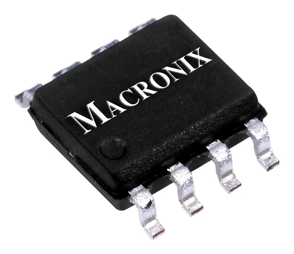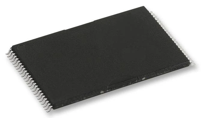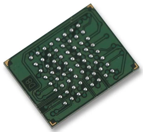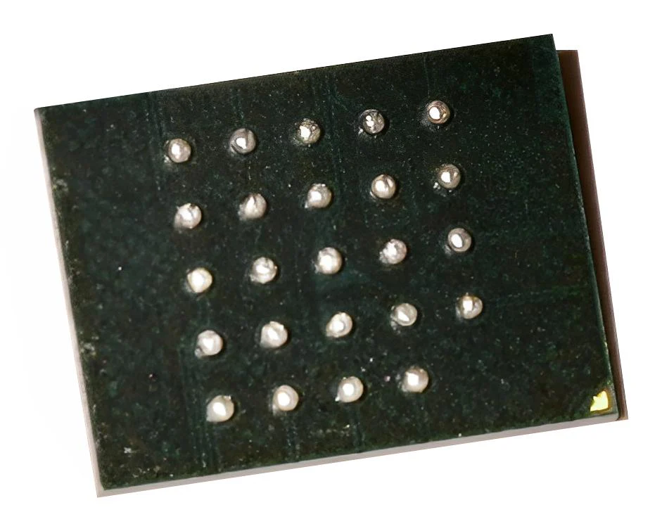
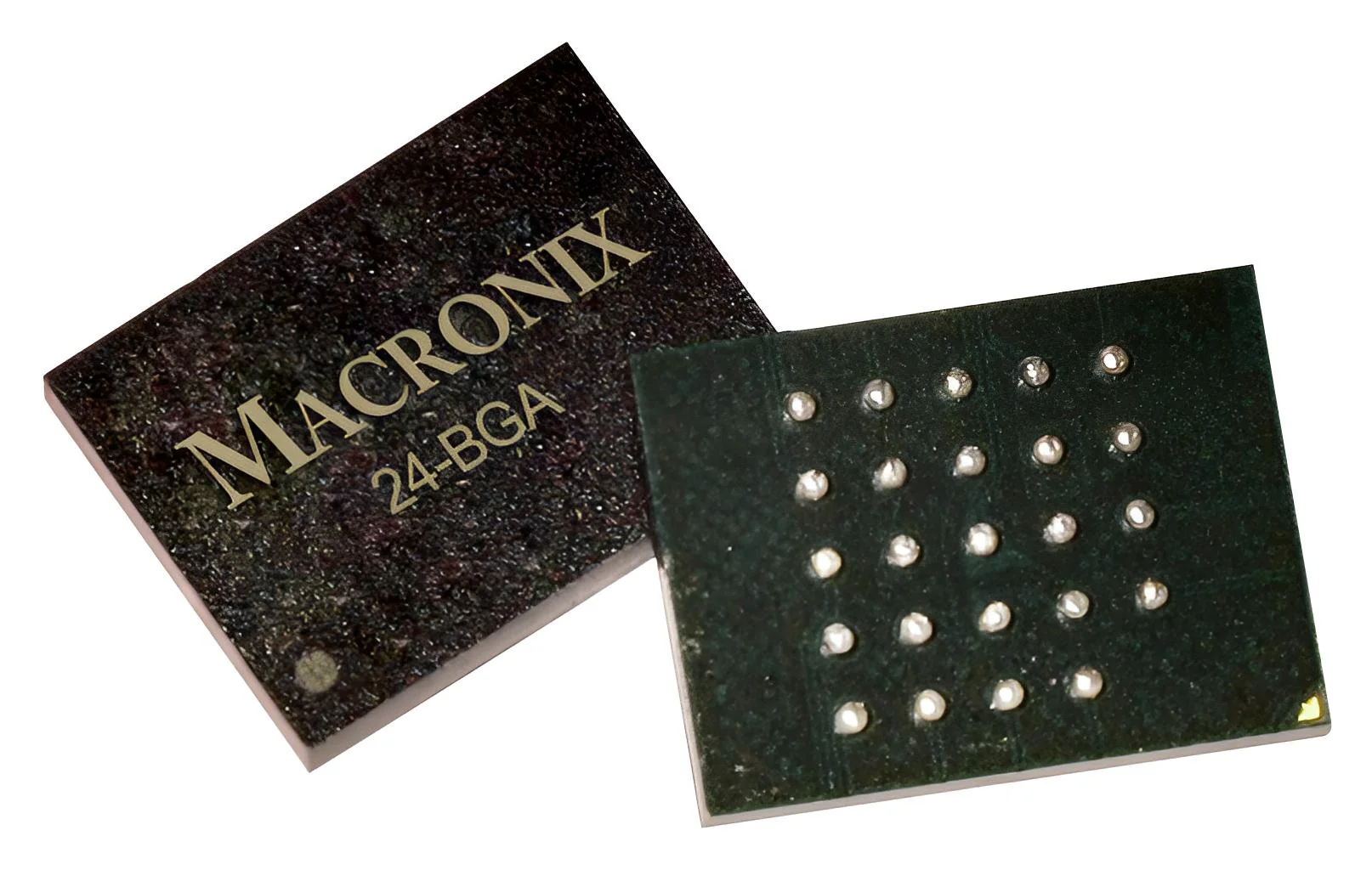
MACRONIX MX25UW25645GXDI00 Flash Memory, Serial NOR, 256 Mbit, 32M x 8bit, SPI, TFBGA, 24 Pins
MACRONIX MX25UW25645GXDI00 Flash Memory, Serial NOR, 256 Mbit, 32M x 8bit, SPI, TFBGA, 24 Pins
Product Overview
MX25UW25645GXDI00 is a 256M-bit serial NOR flash memory, which is configured as 33,554,432 x 8 internally. When it is in two or four I/O mode, the structure becomes 134,217,728 bits x 2 or 67,108,864 bits x 4. MX25U25645G features a serial peripheral interface and software protocol allowing operation on a simple 3-wire bus while it is in single I/O mode. The three bus signals are a clock input (SCLK), a serial data input (SI), and a serial data output (SO). Serial access to the device is enabled by CS# input. When it is in two I/O read mode, the SI pin and SO pin become SIO0 pin and SIO1 pin for address/dummy bits input and data output. When it is in four I/O read mode, the SI pin, SO pin, WP# and RESET# pin become SIO0 pin, SIO1 pin, SIO2 pin and SIO3 pin for address/dummy bits input and data output. The MX25U25645G MXSMIO (serial multi I/O) provides sequential read operation on whole chip.
- Single power supply operation from 1.65 to 2.0 volt for read, erase, and program operations
- Latch-up protected to 100mA from -1V to Vcc +1V
- Support performance enhance mode - XIP (execute-in-place)
- Quad input/output page program(4PP) to enhance program performance
- Typical 100,000 erase/program cycles, 20 years data retention
- Command reset, program/erase suspend and resume operation
- Support serial flash discoverable parameters (SFDP) mode
- Serial clock input, additional 8K bit security OTP
- Ambient temperature range from -40°C to 85°C
- 24-ball BGA package
Product details
Other details
| Brand | MACRONIX |
| Part Number | MX25UW25645GXDI00 |
| Quantity | Each |
| Technical Data Sheet EN |
All product and company names are trademarks™ or registered® trademarks of their respective holders. Use of them does not imply any affiliation with or endorsement by them.
More Images
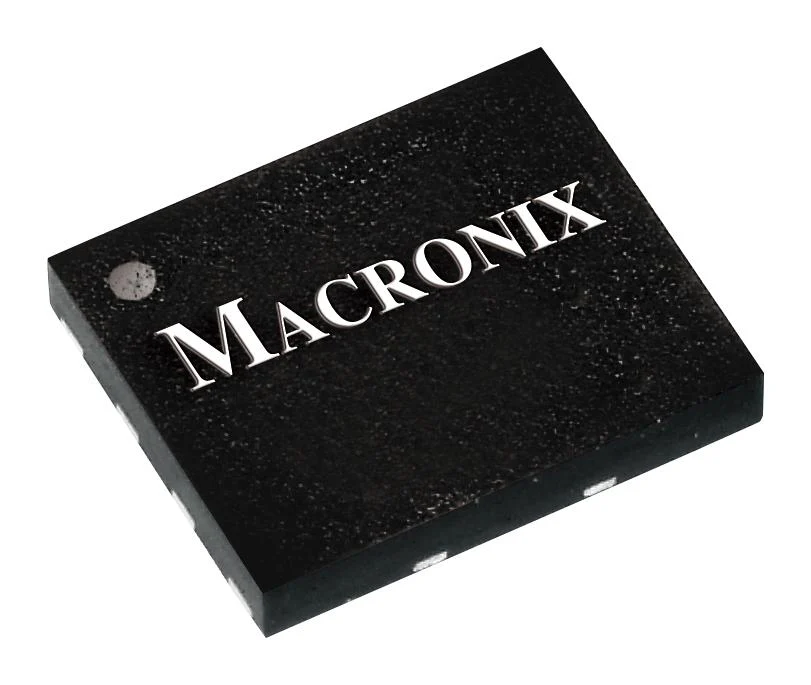
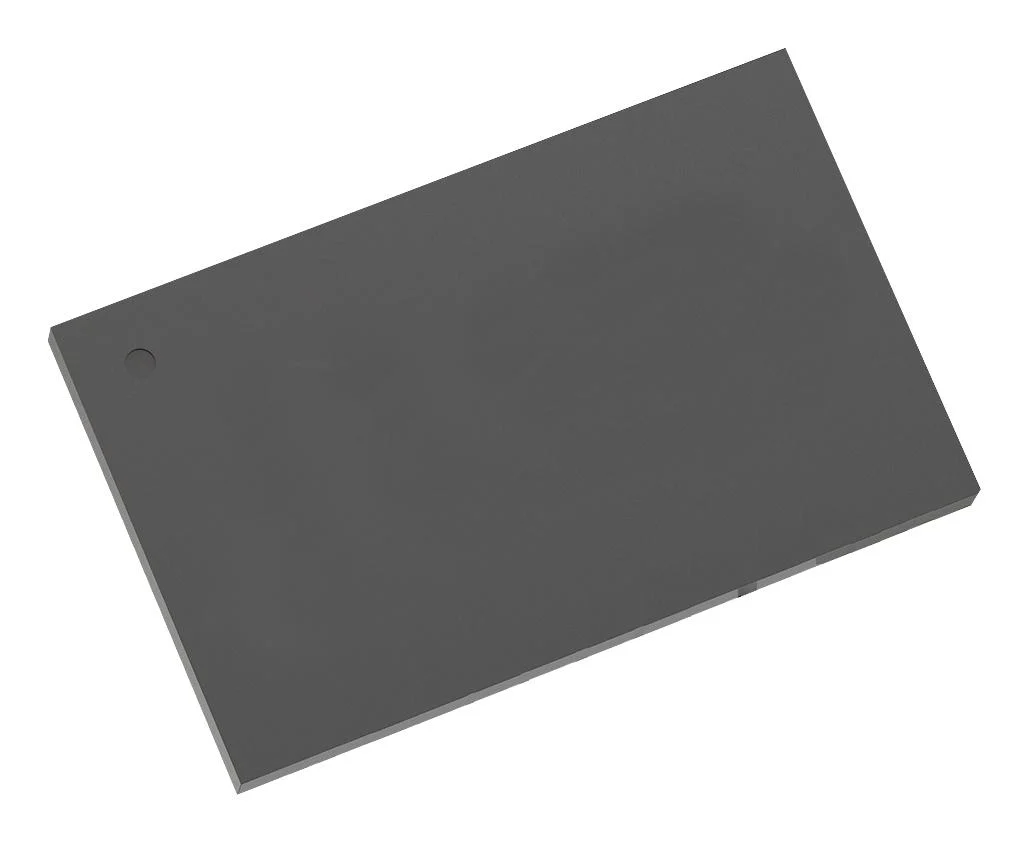
MACRONIX MX25UW25645GXDI00 Flash Memory, Serial NOR, 256 Mbit, 32M x 8bit, SPI, TFBGA, 24 Pins
Product Overview
MX25UW25645GXDI00 is a 256M-bit serial NOR flash memory, which is configured as 33,554,432 x 8 internally. When it is in two or four I/O mode, the structure becomes 134,217,728 bits x 2 or 67,108,864 bits x 4. MX25U25645G features a serial peripheral interface and software protocol allowing operation on a simple 3-wire bus while it is in single I/O mode. The three bus signals are a clock input (SCLK), a serial data input (SI), and a serial data output (SO). Serial access to the device is enabled by CS# input. When it is in two I/O read mode, the SI pin and SO pin become SIO0 pin and SIO1 pin for address/dummy bits input and data output. When it is in four I/O read mode, the SI pin, SO pin, WP# and RESET# pin become SIO0 pin, SIO1 pin, SIO2 pin and SIO3 pin for address/dummy bits input and data output. The MX25U25645G MXSMIO (serial multi I/O) provides sequential read operation on whole chip.
- Single power supply operation from 1.65 to 2.0 volt for read, erase, and program operations
- Latch-up protected to 100mA from -1V to Vcc +1V
- Support performance enhance mode - XIP (execute-in-place)
- Quad input/output page program(4PP) to enhance program performance
- Typical 100,000 erase/program cycles, 20 years data retention
- Command reset, program/erase suspend and resume operation
- Support serial flash discoverable parameters (SFDP) mode
- Serial clock input, additional 8K bit security OTP
- Ambient temperature range from -40°C to 85°C
- 24-ball BGA package
Product details
Other details
| Brand | MACRONIX |
| Part Number | MX25UW25645GXDI00 |
| Quantity | Each |
| Technical Data Sheet EN |
All product and company names are trademarks™ or registered® trademarks of their respective holders. Use of them does not imply any affiliation with or endorsement by them.
Product Information
Product Information
Shipping & Returns
Shipping & Returns
Description
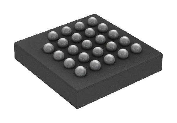
Product Overview
MX25UW25645GXDI00 is a 256M-bit serial NOR flash memory, which is configured as 33,554,432 x 8 internally. When it is in two or four I/O mode, the structure becomes 134,217,728 bits x 2 or 67,108,864 bits x 4. MX25U25645G features a serial peripheral interface and software protocol allowing operation on a simple 3-wire bus while it is in single I/O mode. The three bus signals are a clock input (SCLK), a serial data input (SI), and a serial data output (SO). Serial access to the device is enabled by CS# input. When it is in two I/O read mode, the SI pin and SO pin become SIO0 pin and SIO1 pin for address/dummy bits input and data output. When it is in four I/O read mode, the SI pin, SO pin, WP# and RESET# pin become SIO0 pin, SIO1 pin, SIO2 pin and SIO3 pin for address/dummy bits input and data output. The MX25U25645G MXSMIO (serial multi I/O) provides sequential read operation on whole chip.
- Single power supply operation from 1.65 to 2.0 volt for read, erase, and program operations
- Latch-up protected to 100mA from -1V to Vcc +1V
- Support performance enhance mode - XIP (execute-in-place)
- Quad input/output page program(4PP) to enhance program performance
- Typical 100,000 erase/program cycles, 20 years data retention
- Command reset, program/erase suspend and resume operation
- Support serial flash discoverable parameters (SFDP) mode
- Serial clock input, additional 8K bit security OTP
- Ambient temperature range from -40°C to 85°C
- 24-ball BGA package
Product details
Other details
| Brand | MACRONIX |
| Part Number | MX25UW25645GXDI00 |
| Quantity | Each |
| Technical Data Sheet EN |
All product and company names are trademarks™ or registered® trademarks of their respective holders. Use of them does not imply any affiliation with or endorsement by them.